
Shape Memory and Superelasticity 1 (2015) 3, 286, https://doi.org/10.1007/s40830-015-0029-9
Abstract
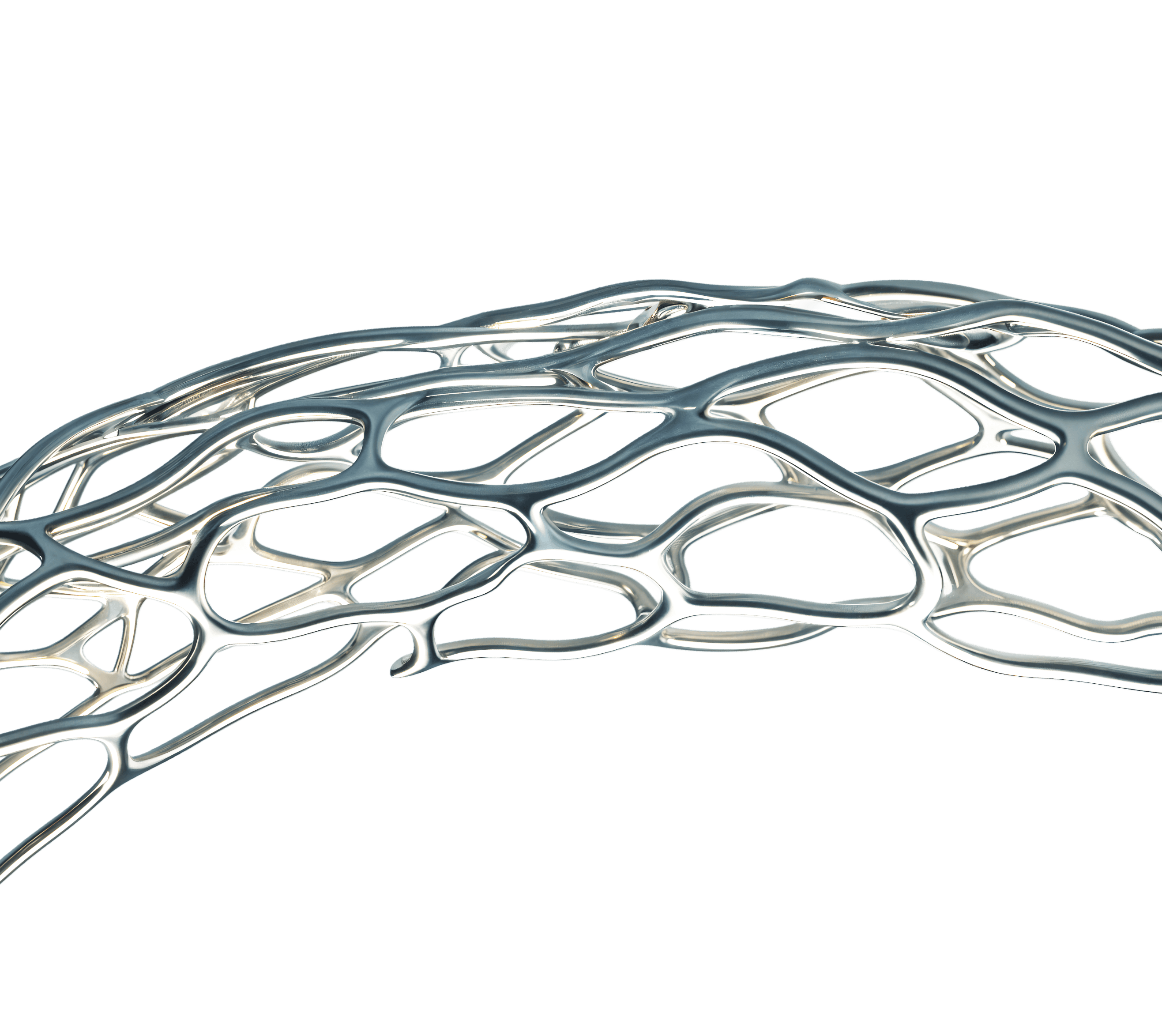
Today, most NiTi devices are manufactured by a combination of conventional metal fabrication steps, e.g., melting, extrusion, cold working, etc., and are subsequently structured by high accuracy laser cutting. This combination has been proven to be very successful; however, there are several limitations to this fabrication route, e.g., in respect to the fabrication of more complex device designs, device miniaturization or the combination of different materials for the integration of further functionality. These issues have to be addressed in order to develop new devices and applications. The fabrication of micro-patterned films using magnetron sputtering, UV lithography, and wet etching has great potential to overcome limitations of conventional device manufacturing. Due to its fabrication characteristics, this method allows the production of devices with complex designs, high structural accuracy, smooth edge profile, at layer thicknesses up to 75 µm. The aim of this study is to present recent developments in the field of NiTi thin film technology, its advantages and limitations, as well as new possible applications in the medical and in non-medical fields. These developments include among others NiTi scaffold structures covered with NiTi membranes for their potential use as filters, heart valve components or aneurysm treatments, as well as micro-actuators for consumable electronics or automotive applications.